hckrnws
DARPA has been thinking about this: https://www.darpa.mil/attachments/AISS_ProposersDay_LeefSlid...
(aside: fascinating example of a US military slide deck, like a 90s fever dream made in Harvard Graphics)
Here’s also a Voices from DARPA episode, which suggests they’ve been funding research since at least 2012: https://blubrry.com/voices_from_darpa/30975140/episode-17-gu...
In terms of ensuring designs are not tampered with seems like watermarking is the direction they’re exploring.
Another fascinating concept was the “silicon odometer” to ensure recycled chips aren’t reintroduced into the supply chain.
Asianometry has a fascinating video on that issue: https://youtu.be/7epnv43jGV8
I'd love to try this some time. Fritzchens Fritz has some other great examples of IR die shots too!
[^1]: https://www.flickr.com/photos/130561288@N04/52465673068/
edit: Oh, bunnie also mentions this in a previous post! See https://www.bunniestudios.com/blog/?p=6656
His images are great! Discovering his photofeed was one of the puzzle pieces that sent me down this path in the first place. I give him a shout-out in the post :)
I only noticed after actually reading the article :^) Lovely work!
Just want to say what a gift Bunnie is to the hardware hacking community. Thank you for all of the work you do helping to push hardware forward in our world!!
Really really cool! Will have to give this a try with my monochrome camera.
I wish there was a bit more detail on possible lenses, its hard to find optics that work well past 1000nm.
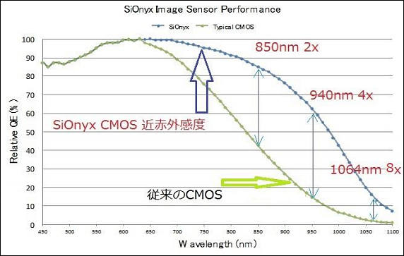
It’s pretty interesting how much the fall off is between 920 to 1070nm - on my camera, 920nm can be exposed perfectly in daylight at around 1/10th of a second, 1070nm needs 4 minutes worth of time to match the same exposure!
Hi! thanks, I'm the post's author.
I had the same concern you have about finding "just the right lens", but was pleasantly surprised to find the $180 camera/lens combo linked in the post worked just fine. In fact basically every piece of optics I had in my lab could pass light at 1050nm, and I have a bit of everything from cheap stuff bought over the counter in Shenzhen to brand-name microscopes. I tried lenses from 6 different vendors and they all worked about the same in terms of passing light (but of course the fidelity of the image scales with cost, better lens tolerances are just more expensive).
My guess is that uncoated glass should be transparent in the 1050nm band, but some lenses have AR coatings that limit the bandwidth. A lot of my lenses do have AR coating (based on the greenish tint I see in the reflections), but I guess the bandwidth of the coating used on most visible-light lenses is just wide enough for 1050nm to slide through.
That's very good to know, thanks for the response! Love your work :)
Looking around, normal industrial (like Pregius) or CCTV (Starvis) sensors are only optimized up into the ~950nm range and drop to near-zero rapidly. The NIR-optimized Starvis seem to be a lot better than normal general purpose sensors already (not sure if this difference comes mainly from different Bayer arrays, in the QE curves these have a very, very distinct hump in the 850-950nm where R/G/B channels seem to have a bandpass). There are some sCMOS cameras (like PCO's stuff [1]) which would seem to be about an order of magnitude more sensitive at 1050 nm than these.
And then there's of course the famed "black silicon". [2]
My money would be on InGaAs sensors [3] being the best in this range. I would also suspect these are subject to funny import/export restrictions, nevermind the price.
[1] https://www.pco.de/scientific-cameras/pcopanda-42-bi/ ~10% QE at 1050 nm [2] https://1.bp.blogspot.com/-wrj9PudX2YM/WkSB-PL-9vI/AAAAAAAAQ... [3] https://www.princetoninstruments.com/wp-content/uploads/2020...
I do wonder what silicon difference a NIR optimized starvis would have vs. the consumer IMX211 silicon, smaller monochrome sensors of the same gen seem fine past 1000NM. Bayer filters would make sense as the actual difference.
I enjoy monochrome infrared photography at wavelengths longer than 1000 nm using a Sigma sd Quattro (no Bayer filter and the sensor IR filter is reversibly user-removable). To reduce exposure times as much as possible, I've been testing an AR-coated near infrared achromatic doublet (AC254-050-B-ML) with a 3D-printed housing to attach it to the camera mount with a manual focusing barrel. The next step is to design a fast double gauss lens that can similarly be assembled from readily available NIR-coated stock lens elements.
I've wondered about doing this a lot! How is the image quality with the doublet? I love the Quattro series of cameras but hate the software personally. I may someday pick up a sd Quattro H...
The center of the image it produces is perfectly sharp, but using a single achromatic doublet as a photographic lens at f/2 necessarily produces significant eighteenth-century softness as you move out to the edges. This image [1] taken to demonstrate that red wine (left) is clear and nearly as transparent as water (right) in the near infrared provides a decent example of how the images it produces wide open soften outside the center much more quickly than modern commercial camera lenses which typically don't lose sharpness at maximum aperture until the corners.
However, the sd Quattro is sensitive enough from 1000 nm - 1100 nm that I can take handheld shots outdoors on a sunny day while stopped down to f/5.6, and the smaller aperture gives more consistent sharpness across the frame. It also only takes a few seconds exposure on tripod to capture astrophotography of red giant stars that emit significant infrared like Betelgeuse.
Incidentally, the original reason I wanted an infrared-sensitive camera and a 1000 nm long pass filter was to photograph stars in the sky during the middle of the day, taking advantage of the quartic dependence on wavelength in Rayleigh scattering to remove the overpowering brightness of the sky.
[1] https://alexbock.github.io/blog/nir-examples/near-infrared-8... (note: this image used an 850 nm long pass filter rather than 1000 nm but was taken with the same doublet described before)
Comment was deleted :(
>How Does It Work? Silicon goes from opaque to transparent in the range of 1000 nm to 1100 nm (shaded band in the illustration below). Above 1100 nm, it’s as transparent as a pane of glass; below 1000 nm, it rapidly becomes more opaque than the darkest sunglasses.
So expect to see more epoxy blobs on top of chips.
There’s a reason these chips are left open. Thermal performance for example might tank if they tried to epoxy those.
I wonder if you could apply photogrammetry processes to this to result in a higher resolution image by shifting things around ever so slightly. Creating a point cloud and getting height data to do closer analysis would be cool, but not sure how light scattering would affect this.
IRIS in the title should be all-caps as it's an acronym; Lowercasing the final letters made me think this was going to use some weird quirk of the human iris.
That's a convention that varies from one region to another. For instance, in the UK it's normal to write initialisms in all caps (e.g. CNN or the FBI) but not acronyms (e.g. Nasa, Opec, or Geico).
This is really cool. What kind of wavelength would be needed to actually 'see' stored data inside silicon and be able to read that out?
It doesn't really work that way, data in silicon is largely stored with charge - if the photons are fat enough to bounce off that charge they're also likely to erase it
Just adding on to taniwha's correct comments -- it is possible to indirectly image the charge using thermal stimulation of the laser to induce the Seeback effect. The local heating will cause the current consumption of the chip to shift ever so slightly in a fashion that's dependent on the state of the transistor's bias. [1] is where I first read about the technique.
> if the photons are fat enough to bounce off that charge they're also likely to erase it
Isn't this how EPROMS are erasable by UV light?
yeah exactly
I wonder if the technique used for inspecting solar silicon could work here. Just apply power and check its IR emissions.
I forget the name it has, but that is a technique used to examine silicon — all the PN junctions in the logic will emit light when they pass current. CMOS logic doesn't have very many (forward-biased) junctions though. IDK if the technique is still useful there.
Crafted by Rajat
Source Code